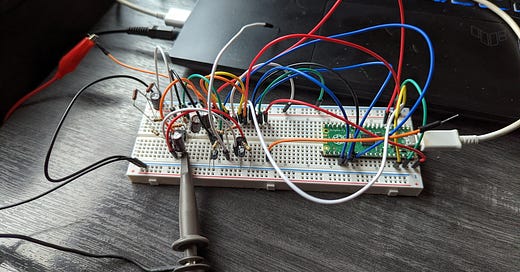
I’ve been chipping away at the design of the Project Yamhill front panel PCB over the last few weeks, but it’s taking a bit of time since it’s the most complex circuit board that will be designed for this endeavor. Most of the microcontroller and LO circuitry have been worked out. Since all of those things are derived from circuits I’ve previous used, I’m fairly confident they will work just fine (except the 4.0” LCD that I chose, which is why I ordered one and breadboarded it to the RasPi Pico right away so I could confirm it world work as expected). These last few days, I’ve laid out a preliminary design for the AF amp system and breadboarded a part of it.
Let’s talk a bit about the design decisions that I’ve made for the AF chain. There are quite a few good audio ICs available from TI that handle the final audio stage nicely, including having enough output power to drive a small speaker, have the ability to switch between a speaker and headphones gracefully, and can be put into shutdown mode with no popping or artifacts. Rather than reinvent the wheel, it makes sense to use one of those, so in this case I chose a LM4875.
I’m not going to use the adjustable gain feature of the LM4875 itself, since I want to be able to generate a sidetone that has a volume level independent of the receiver volume. Instead, the sidetone will be fed in parallel to the LM4875 input, along with the audio from the receiver audio chain. A standard AF gain pot will be used to control the audio level from the receiver, just before the LM4875 input. The LM4875 volume/shutdown pin will be connected to a Pico GPIO with PWM so that it can be controlled from the microcontroller if necessary, although I have no plan to do so during the initial iteration of this design.
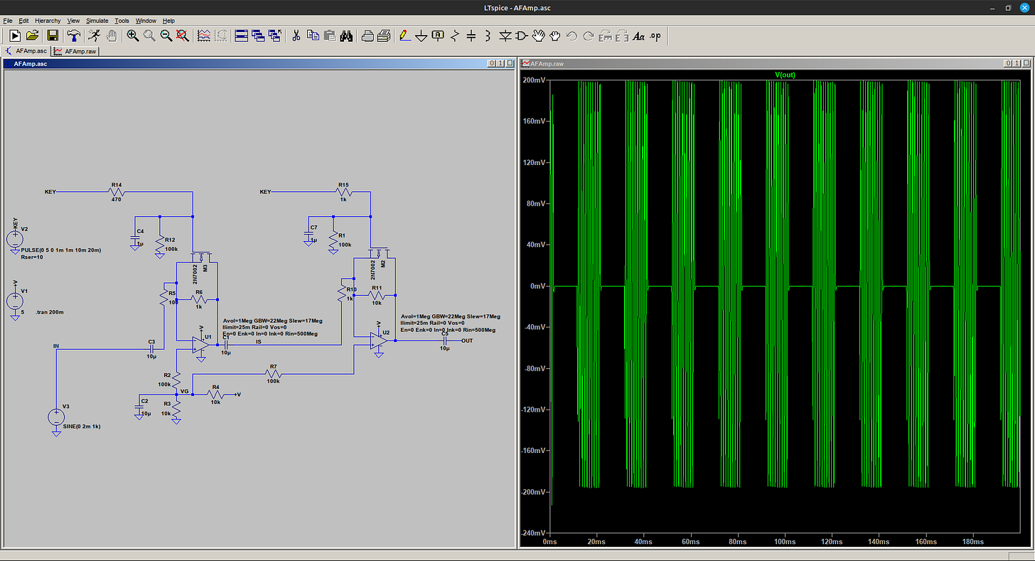
Since the LM4875 is a power amplifier and gives about 20 dB of audio gain, the audio stage needs a preamplifier to give another 40 dB or so of gain in order to meet the target of the specifications from the architecture document. A classic two-stage op amp circuit seems to fit the bill nicely here, and there’s very little to be said about the above circuit other than I’m sure you’ve seen it in plenty of designs. The real challenge is in designing a mute circuit for such an amplifier that will work effectively, responsively, and without switching artifacts.
For this design exercise, I dusted off LTSpice (haven’t used it in years, sadly) and virtually tried out various common mute methods, but I was not happy with any of them. A lot of them involve a series and/or shunt switching element made out of a JFET or MOSFET transistor that is in-line with the output of the amp. The big problem with these circuits is that they create transients in the AF signal path during switching, I believe because of the DC bias of op amp virtual ground. I bet these circuits work fine in a dual-supply op amp circuit, but they’re not suitable for here. Going back over revered literature, specifically Experimental Methods in RF Design, I did notice one mute circuit that looked promising. A JFET was used in parallel with the feedback resistor in the op amp, shunting it out when activated. I decided to try to recreate this circuit with a MOSFET instead of a JFET, as you can see above. The nice thing about this scheme is that the both the drain and source of the MOSFET are at the virtual ground DC bias level, so there are no impulses created during switching that I can see in the LTSpice simulation and can see from looking at the real circuit with an oscilloscope. I can feed a very large signal into the input (far larger than it would ever see in real use), and can’t hear a bit of the signal leak through when the mute is applied, just a bit of hiss from the op amp. I think that’s a nice first pass at this circuit.
Welcome New Subscribers
I’ve noticed that I’ve received quite a few new free subscribers lately. Welcome aboard this journey and thank you!
Substack seems to have some pretty good analytics, but I can’t discern any particular referrer for the new subscribers from last few days. If someone did recommend my Substack, thank you.
If you haven’t subscribed yet, please consider doing so. You can subscribe for free to receive every new post in your email inbox, and Substack is very good about respecting your privacy and not spamming you with additional crap.
Sadly, I’m seeing reports that Twitter is shadowbanning links out to Substack, which is squelching the reach of this platform. If you find these posts useful, please share with others, I guess on non-Twitter platforms.
Further Thoughts on the Ender-5 S1
I had mentioned in my last post that I was happy with the Ender-5 S1 so far, but was having some difficulties printing PETG, which is the filament that I plan to use for the backplane design.
After getting a bit frustrated, I was able to figure out most of my problems and can now print in PETG pretty well. I did a combination of things, including:
Calibrated the extruder stepper in Klipper
Purchased a filament dryer (important since PETG is hygroscopic and I’m printing out of what is essentially a tent, and right now it’s very humid)
Replaced the stock PC build surface for PEI build plate (what an upgrade!)
Resetting my slicer settings and then tweaking one parameter at a time
I think all items were helpful, but the last one was the most important. My print profile got way into the weeds, and who knows what I screwed up there along the way.
The resulting print looks decent, with only some minor problems like zits and a little bit of stringing. The printer might still be overextruding a bit. I imagine that I can do a bit of tweaking to reduce those flaws further, but this is certainly good enough for purpose. The best thing is that I was able to realize the time savings that I was hoping for when I took the leap of purchasing the Ender-5 S1 with the Sonic Pad. To get a half-decent print from my old Ender-3, it took a bit over 13 hours to print the section in the photo above. With the new rig, it took just a smidge over 6 hours, a bit less than half of the time. As I get well into middle age, I realize just how important that time is, so spending a bit of money to reclaim a significant amount of time is a wise investment.
Up Next
I can’t guarantee this, but my goal is to have the initial front panel circuit design finished in about a week so that I can present it here. I’m eager to start sending some design files to the PCB fab and get to building some stuff soon!


